Hat Creek Info Please
- Desired info as of November 11, 2007
- General Items
- Data Path
- BEE2 DSP Platform
- ATA Hardware links & notes (mostly aimed at electronic processing room
General Items
DATA PATH
BEE2 DSP Platform
Major heading Minor heading Comments
Name of control building, various rooms? . .
. repair shop .
. raised floor electronics racks .
. "mission control" .
Array scheduling? paper for now?? . .
Array control - setup . .
. beam target selection .
. individual target selection .
. individual data path scheduling .
. base local oscillators .
Array control -running . .
. az,el to post head - some odd name .
. course delay control, period?
BEE mentions double buffering
late status? .
. fine delay control, period? .
Calibration (42x2) . .
. bore sighting .
. phase, gain .
. base location, location of front-end .
. base transit time .
Time . .
. sidereal clock .
. GPS clock, ? civil clock UT1, UT2, GMT, ??? .
. when/where time tagging, sidereal/civil? .
field power distribution . .
control house power distribution . .
Function
Color coding [analog], [digital]
Unit Name Front connector(s) color Connectors(s) data rate
. Links/notes back connector(s) connectors(s) data rate
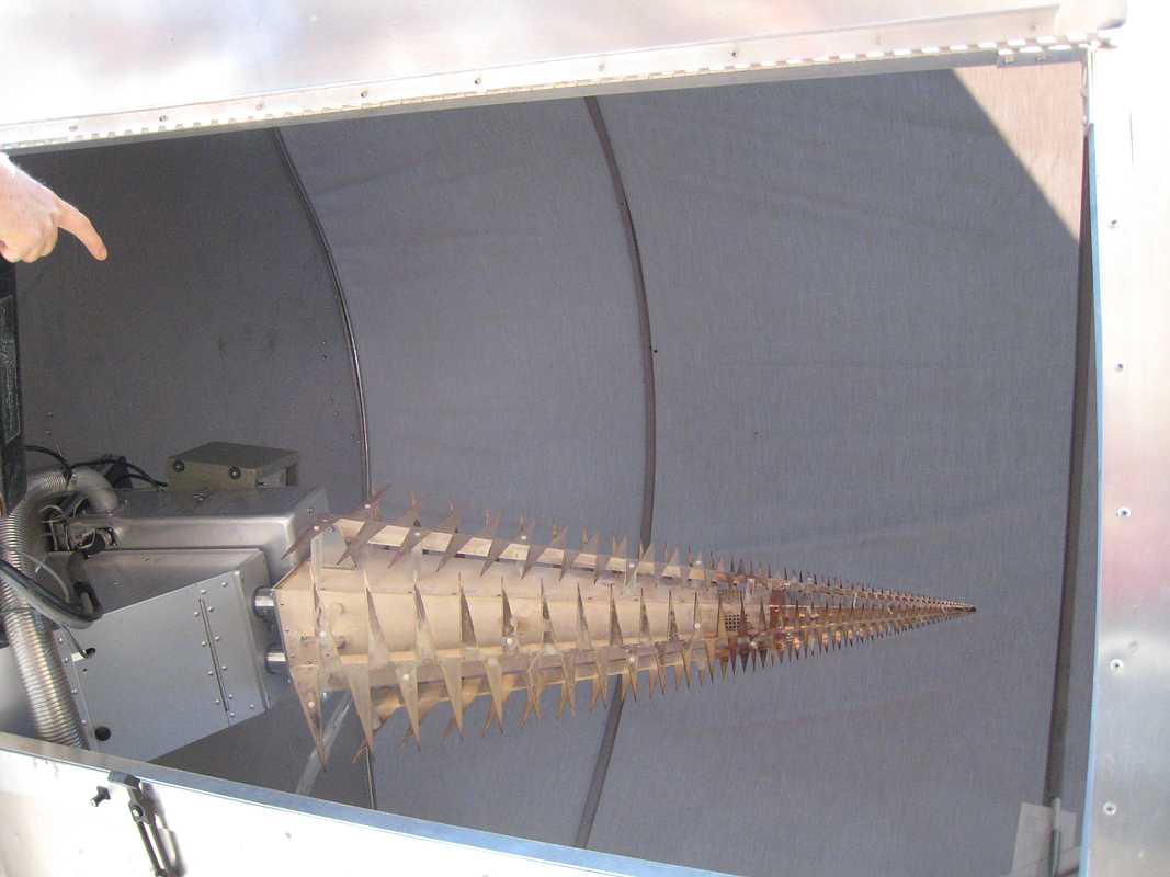
LogPeriodic => .
.
. . . .
300? ohm wire pair => . . .
. . . .
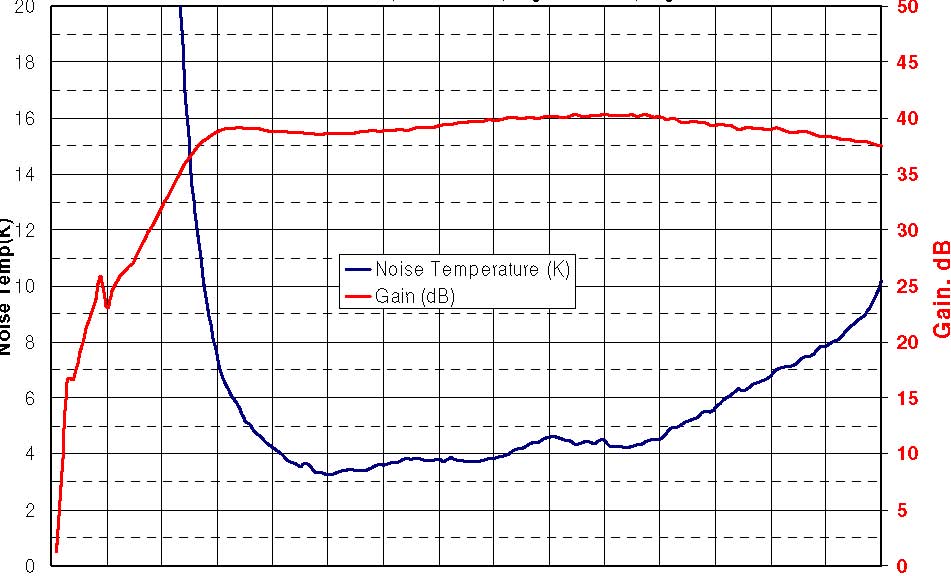
chilled Low Noise Amplifier =>
comments from http://webmail.jb.man.ac.uk/ pulsar2007/talks/april3/Jones.pdf
Caltech-Developed Cryoginic LNA's Caltech EE has delivered 160 LNA's to other Research Centers during the past
4 years. This does not include LNA''s for the 350 element Allen Telescope Array or the 64 element U. of Arizona
Submillimeter Camera
http://webmail.jb.man.ac.uk/ pulsar2007/talks/april3/Jones.pdf
.
. . . .
coax => .
. .
. . . .
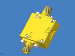
amplifier => .
![]()
.
. . . .
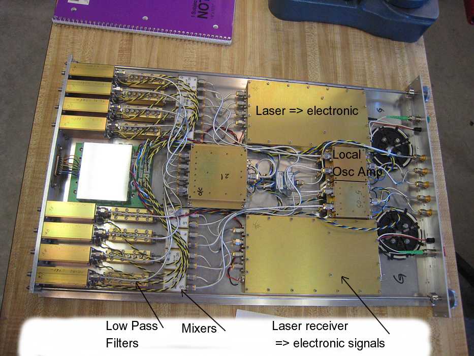
laser transmitter => . Part of above amplifier board .
. . . .
fiber optic => . Part of above amplifier board .
. . . .
fiber optic via node => .

.
. . . .
fiber optic in computer room => .

.
. . . .
laser receiver => .
.
. . . .
amplifier?/equalizer? => . see above image .
. . . .
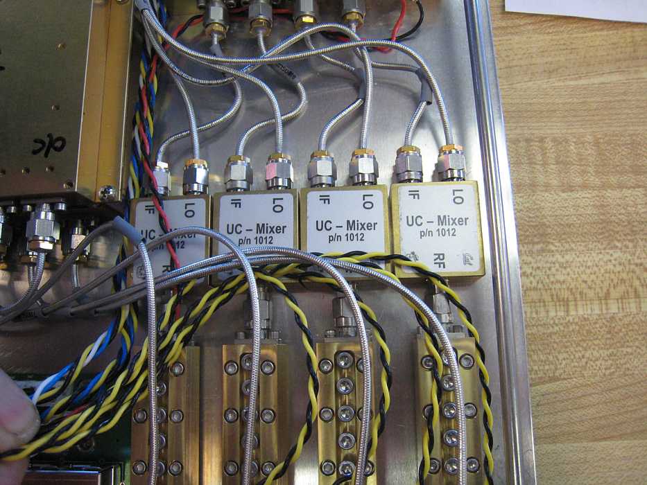
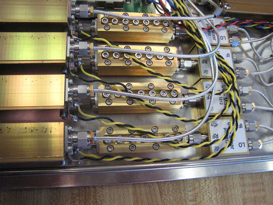
RF Mixer => .
.
. . . .
LowPassFilter => .
.
. . . .
ADC => I think the amplified? lowpass signal goes to the ADC in this BEE2?
.
. . .
DigitalDownConverter => . . .
. . . .
Coarse Delay DigitallyControlledFIFO => . . .
. . . .
Fine delay filter => . . .
. . . .
ADC => . . .
. . . .
to non-linear(s), or to correlators? . . .
. . . .
useage? -> storage (time tagging?) . . .
. . . .
On-line usage? . . .
. . . .
On-line calibration tracking? . . .
. . . .
--------- .
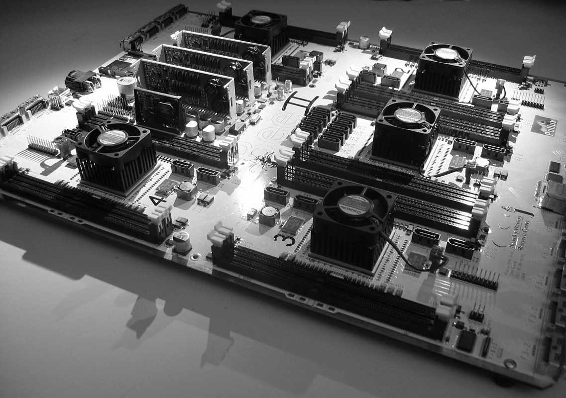
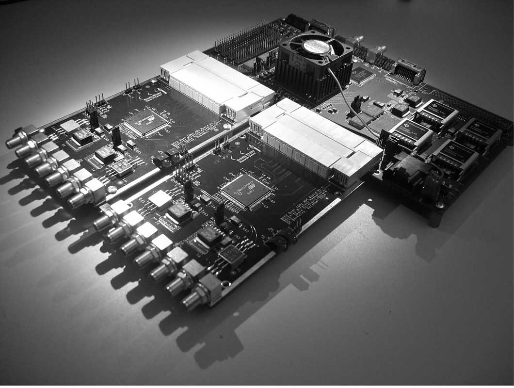
BEE2 DSP Platform
The spectrometer is built on a Berkeley Wireless Research Center (BWRC) BEE2 (Berkeley Emulation Engine) platform.
Originally designed for high-end reconfigurable computing applications such as DSP and ASIC oriented towards radio astronomy
applications was developed as a collaboration between the BWRC, the UC Berkeley Radio Astronomy Lab, and the UC Berkeley SETI
Group. The system consists of three main components:
BEE2 source
ADC source
iBOB source
ADC board Analog data is digitized using an Atmel AT84AD001B dual 8-bit 1Gsample/s ADC. The ADC can be driven with
either single-ended or differential inputs, and can digitize either 2 streams at 1Gsample/s or a single stream at 2Gsample/s.
The board is designed to mate directly to an IBOB board for high-speed serial data I/O.
from https://wikio.nrao.edu/pub/CICADA/CicadaNotes/cicadaNote003.pdf
Clock The ADC board takes a high speed clock (100 to 1000 MHz) as input for
controlling the data sample rate. The IBOB board clock will be one quarter of the input ADC
clock rate.
1 PPS The absolute time reference is based on a GPS referenced I Pulse per
second synchronization pulse. This pulse is used to measure the offset between the IBOB
board internal clock counters and absolute time.
I Channel The astronomical signals are provided to the IBOB in the IF frequency
range 500 to 1000 MHz. The input signals are bandwidth limited to avoid aliasing of the input
signals.
Q Channel Similar to I Channel.
purpose:
	ADC Board FAQ   http://bee2.eecs.berkeley.edu/wiki/AdcFaq.html
	I+, Q+ and clk_i inputs
        Photo -
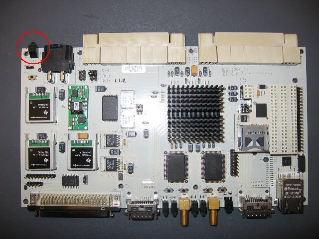
iBOB board IBOB (InfiniBand BreakOut Board) boards allow a variety of I/O cards to provide data for packetization
onto the InfiniBand protocol. Each board provides 2 Z-DOK+ connectors for I/O card attachment, and 2 CX4 InfiniBand connectors
for interface to BEE2 boards. Data serialization is done by a Xilinx XC2VP50 FPGA. The FPGA provides 232 18x18-bit multipliers,
2 PowerPC cores, 4176Kb of SRAM in addition to 36Mbit of on-board ZBT SRAM, and over 53,000 logic cells, allowing the
purpose:
     	IBOB Board FAQ  http://bee2.eecs.berkeley.edu/wiki/IbobFaq.html
        Photo -
 	IBOB 	 ADC ports http://bee2.eecs.berkeley.edu/wiki/IbobFaq.html
BEE2 Board The BEE2 board integrates high computational density with high-speed I/Os. Compute power is provided by
its 5 Xilinx XC2VP70 Virtex-II Pro FPGAs (Field- Programmable Gate Array), each containing 328 18x18-bit multipliers,
2 PowerPC cores, 5904Kb of SRAM, and over 74,000 logic cells. In addition, each FPGA can be provided with up to 4GB of
DDR2-SDRAM. External interfaces are available through 10Gb/s InfiniBand connections on the user FPGAs, as well as 100Mbps
Ethernet and RS232 serial ports through the control FPGA.
Design goal, reconfigurable FPGA based supercomputer
    ATA purpose:  FIFO/DelayLine controller, communication,
               programmable DigitalFrequencyConverter

        Photo -

     History BEE => BEE2 (2004) http://inst.eecs.berkeley.edu/~cs152/fa04/lecnotes/bee2_cs152_120204.pdf

    BEE2 Documentation   http://bee2.eecs.berkeley.edu/wiki/BEE2wiki.html

    BEE2 Quick Start    http://bee2.eecs.berkeley.edu/wiki/Bee2QuickStart.html

    BEE2 Board FAQ    http://bee2.eecs.berkeley.edu/wiki/Bee2Faq.html?action=PackagePages

    Memory http://bee2.eecs.berkeley.edu/wiki/Bee2Memory.html
http://bee2.eecs.berkeley.edu/wiki/Bee2QuickStart.html#head-bb352cb385f2174d3cf9ee4a97cbf3ed92b93523
   has picture
	- runs of own 200 MHz clock,
		 uses Async Command FFIOs => onboard DDR2 controller => DIMM
	- multiport Access
		modes include round robin and burst
	- each BEE2 module has five Virtex-II Pro 70 FPGAs
             each to four independent 1 GB ram modules
	- bus width = 72 bits to permit ECC
  All links to http://bee2.eecs.berkeley.edu/module/
       yield a web page with all dead links  :-((

  Bee2Setup   http://bee2.eecs.berkeley.edu/wiki/Bee2Setup.html

  Bee2TestSuite http://bee2.eecs.berkeley.edu/wiki/Bee2TestSuite.html

  Bee2Binaries  http://bee2.eecs.berkeley.edu/wiki/Bee2Binaries.html

  BEE2 IP Core Documentation   http://bee2.eecs.berkeley.edu/wiki/Bee2Cores.html

  BEE2 Errata   http://bee2.eecs.berkeley.edu/wiki/Bee2Errata.html#head-51b00a6b81c4d4289612ba09bd4a58f6e79f3702
software tools .
MSSGE MSSGE stands for Matlab/Simulink/System Generator/EDK toolflow.
http://bee2.eecs.berkeley.edu/wiki/MssgeFaq.html
BEE2 Control FPGA:
plb_ethernet_v1
opb_uart_16550
IBOB:
opb_ethernetlite
Common:
XAUI s
Block Creators purpose:
Block Creators FAQ http://bee2.eecs.berkeley.edu/wiki/BcFaq.html