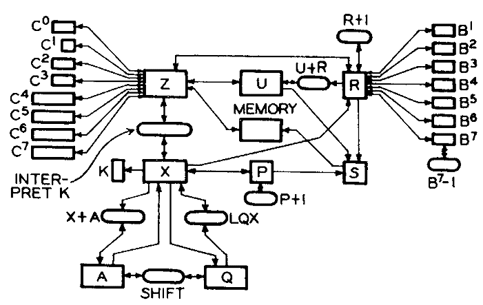
Fig. 1. Block diagram showing the inter connections of the four sections
Go to On Line Documents, Go to Go to Antique Computer home page
| J. E. THORNTON | M. MACAULAY | D. H. TOTH |
| J. E. THORNTON, M. MACAULAY, and D. H, TOTH are with Remington Rand Univac, Division of Sperry-Rand Corporation, Saint Paul, Minn. |
THE Univac M-460 is a computer of advanced design from both the logical and engineering standpoints. It is the intent of this paper to describe its more interesting features.
The Univac M-460 computer is a large scale high-speed general-purpose digital computer especially suited to rapid, complex processing of large quantities of data. The computer is a parallel, single address computer with fixed point, one's complement binary arithmetic. A computer word in the M- 460 is 30 binary digits in length with the provision for treating the two 15-bit halves independently, if desired. The memory section has a capacity of 32,768 30-bit words with a cycle time of 8 microseconds, and a read access time of 2.5 microseconds.
Special advanced logical features give the M- 460 a great deal of programming flexibility. From the standpoint of the number of instructions required for a given operation, the effect is much as if two-address logic were employed.
For purposes of discussion, the computer may be divided into four sections: control, arithmetic, input-output, and memory. The block diagram of Fig. 1 shows the interconnections of each of the four sections. The main registers of the computer are shown by rectangles. Some of the principal functions of each section are indicated within the roundedged blocks.
Fig. 1. Block diagram showing the inter
connections of the four sections
The control section includes a 30-bit instruction register U, a 15-bit program address register P, seven 15-bit address modification registers, B, through B7, and a 15- bit auxiliary register R. A computer instruction is executed by first acquiring an instruction word from the memory location designated by the P register and then performing a number of operation sequences controlled by the instruction register U. Normally the content of the P register is advanced by one count for each instruction so that instructions are executed in numerical sequence. Program branching may be performed by changing the contents of the P register in jump instructions. A special feature of the control section permits program branching by another method. A skip designator, active in most instructions, permits an extra one-count advance of the P register if certain arithmetic criteria specified in the instructions are met. Thus the next sequential instruction may be conditionally skipped.
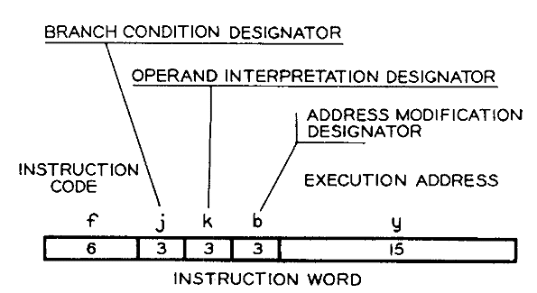
Fig. 2. Organization of the instruction word
The organization of the instruction word is shown in Fig. 2. There are 62 basic instructions designated by f, the upper 6 bits of the instruction word. These basic instructions are supplemented by three designators j, k, and b and a basic execution address y. In understanding the execution of an instruction, each of the following four main sequences should be considered:
Read Next Instruction. An instruction word is acquired from memory during the A sequence and is transferred to the U register. While the memory restore cycle is being completed, a modification is made to the lower half of the instruction. The basic execution address is modified by the addition of the content of one of seven B registers specified by the b designator of the instruction. This modification is complete by the time the instruction memory reference is finished. If the b designator is zero, no modification results.
Read Operand. An operand is obtained during the B sequence, the source of the operand being specified by the execution address as previously modified by the b designator. The operand interpretation designator, k, is active during the B sequence. Depending upon the the value of k, the operand may be the lower order 15 bits of the instruction word, the upper or lower 15 bits of a memory location, or the full 30-bit word contained in a memory location.
Arithmetic. Any arithmetic to be performed in the instruction is completed during the C sequence. No memory reference is required in this sequence.
Store Operand. If the result is to be stored, this storage action occurs during the D sequence. In the D sequence the operand interpretation designator is again used. Depending upon the value of k, the result may be stored in either half or all of a memory location, or the result may be transmitted to the accumulator or Q register.
The last designator active in the instruction is the branch condition designator j. This designator is used in three ways involving the B, C, and D sequences. First of all, most instructions utilize the j designator to specify whether the next sequential instruction is to be skipped as a result of the condition of the accumulator or Q register at the end of the current instruction. Second, the jump instructions utilize the j designator to specify whether a jump is to be per- formed depending on the condition of the accumulator or Q register. Finally, in- structions requiring the use of a B or C register utilize the j designator to specify the particular B or C register to be employed.
The sixty-two basic instructions may be classed into 6 groups which include instructions involving data transfer, arithmetic, logical operations, jumps, indexing, and special operations. Instructions are basically single-address and are supplemented by the previously described designators. The special instructions include repeat, initiate input buffer or output buffer, compare, and masked comparison. Instruction execution times range from 11 microseconds for add constant to 130 microseconds for divide. Typical instruction time is 20 microseconds.
The arithmetic section of the Univac M-460 comprises three 30-hit registers, the accumulator, the Q register and the X register. Fixed-point binary arithmetic including add, subtract, multiply, and divide is performed in these registers. Double-length products obtained from multiplication instructions and double-length dividends before division instructions are held in the combined accumulator and Q register, used as one 60-bit register. The least significant 30 bits reside in the Q register, and the most significant 30 bits are held in the accumulator. The accumulator and Q register have high-speed shifting properties. The contents may be shifted right or left independently or as one 60-bit register. A shift of 30 places requires a total of 3 1/2 microseconds. Operands are always transferred to and from the arithmetic section through the X register.
The memory section is a coincident current, random-access ferrite-core memory of 32,768 words with a 30-bit data register Z and a 15-bit address register S. The other three sections of the computer have direct independent access to memory. Instructions, operands, and input-output data may be stored in any desired location in the memory. One complete memory cycle comprising a read and write operation is performed in 8 microseconds, the read access time being 2.5 microseconds. Since the memory employs destructive read-out, a read-memory reference is always completed by rewriting the information which was previously read. Similarly, a write memory reference is always begun by reading the contents of the designated memory location, thus clearing that location before writing. All memory references, either read or write, require a compete memory cycle and the same sequencing mechanism controls both functions.'
An important characteristic of the Univac M-460 is the versatility of its input-output section. Seven parallel registers are provided for the transfer of data to and from the computer. A total of 30 channels are available without additional switch gear; eighteen channels for input and twelve channels for output. One channel of each register may be activated at any one time. Furthermore, each channel may be connected to a number of external devices.
The concurrent operation of a number of external devices requires control communication as well as data communication. One of the seven registers of the input-output section is designated as the function register C3. It performs the control communication function. For example, a transfer of data between an external device and the computer often requires deactivating all other devices on the assigned channel and activating the desired device. Other representative requests by the computer could be start motor, stop motor, advance, transmit, receive, etc. Requests may also come to the computer from the external device through the function register. Computer handling of such requests can be divided into two groups, scan and interrupt. In the first group, scan, the computer program examines the input channels of the function register periodically to determine whether a request has been made. In the second group, interrupt, the com- puter program is interrupted by means of an interrupt line provided on each of the input channels to the function register. This interruption causes the computer to halt its current program and to jump to a special interrupt routine. Special precautions are taken to prevent any conflicts between multiple interrupts, loss of current data, etc.
Another important feature of the input-output section is its ability to transfer data to and from memory independently of, and concurrently with, arithmetic operations. Data may be transferred by direct program transfer or by an independent buffer control, which is initiated by the program. The initiation of. a buffer operation on a given input-output register establishes an initial memory address and a terminal memory address. Thereafter, data is transferred between memory and the external device at a rate controlled by the external device. The initial memory address is advanced for each transfer and compared with the terminal address. When the two addresses are equal, the Buffer operation is made inactive for that register until initiated once again by the computer program. Six such buffer operations may be operating concurrently using a built-in priority system, which allows the highest priority transfer to proceed at any instant.
A lockout system is employed to properly sequence requests for memory references since a buffer operation and the main computer program might request the simultaneous use of memory. The maximum input-output rates range up to over 50,000 words per second depending upon the communications structure. Since the words are 30-bits long, a maximum rate of over 1.5 million bits per second is possible.
An additional feature of interest is the inclusion of a real-time clock facility. Real time to the nearest millisecond is available to crystal oscillator accuracy.
It is surely apparent at this point that the Univac M-460 computer is a powerful computer having high-program speed, a large high-speed memory, and a versatile input-output system. The remainder of this paper discusses the construction and design methods employed.
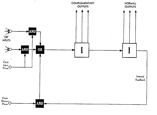
Fig. 3. Block diagram of the logical building block
The logical sections of the M-460 are implemented with transistor building blocks shown in block diagram form in Fig. 3. Each building block is made up of two inverters, which provide the normal and complementary outputs, plus "and-or" logical inputs to the first inverter. All logical decisions are gated by a square-wave clock at the entry to each building block. A feedback path is provided from the second inverter to the first and is gated by the opposite phase of square-wave clock. The operation of a building block follows a continuous 2-phase sequence:
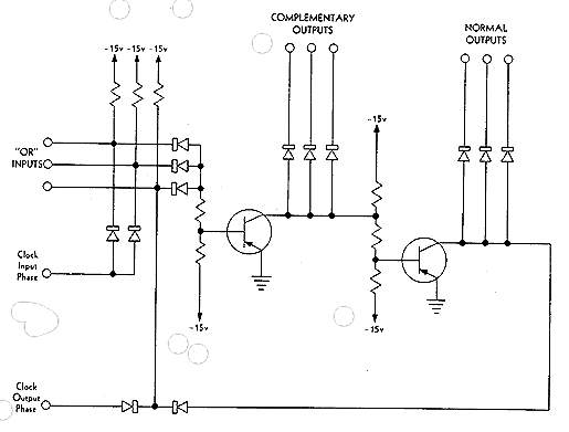
Fig. 4. Schematic of the logical building block
Mechanized design methods, described in a previous paper, were used with this building block. These mechanized design methods made possible a very short design and development period. For one thing, the ERA 1103 (Univac Scientific) computer was programmed to simulate, verify, and correct the logical design of the M-460. Even more important, the 1103 was used to provide optimum building block placement, complete wiring tabulations, chassis maps, cross-reference tabulations, and parts lists.
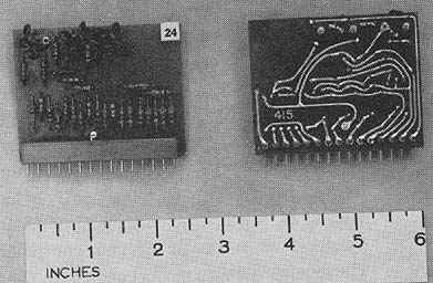
Fig. 5. Logical building block components mounted on cards
The logical building blocks are constructed of, fibre-glass cards with an etched circuit of copper foil bonded to one side. The dimensions of the cards are 2 inches by 2.5 inches. As shown in Fig. 5, components are mounted on the side of the board opposite the wiring. A 15-pin connector at the base of the card allows each building block to be easily removed. These logical building blocks are mounted on a flat chassis, shown in Fig. 6, whose dimensions are 28 inches by 30 inches. Each chassis contains its own power supply and 2-phase clock "slaves."
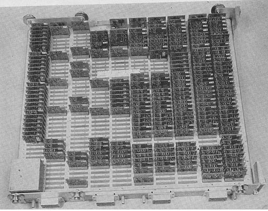
Fig. 6. Logical building blocks mounted on a flat chassis
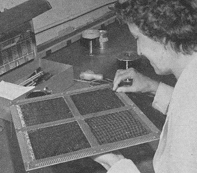
Fig. 7. The memory section containing a coincident-current magnetic core memory
The memory section contains a coincident- current magnetic core memory made up of ferrite memory arrays, shown in Fig. 7, and transistor building blocks. Memory current drive of 0.4 ampere is obtained by using high- current germanium transistor switches. The complete memory is divided into five separate memory chassis, one of which is shown in Fig. 8. The memory chassis are identical in size to the logic chassis. Each memory chassis contains its own power supply and is completely interchangeable with the other four memory chassis. Considerable effort was devoted to the orientation of memory arrays and transistor building blocks on this chassis in order to obtain an optimum electrical arrangement.
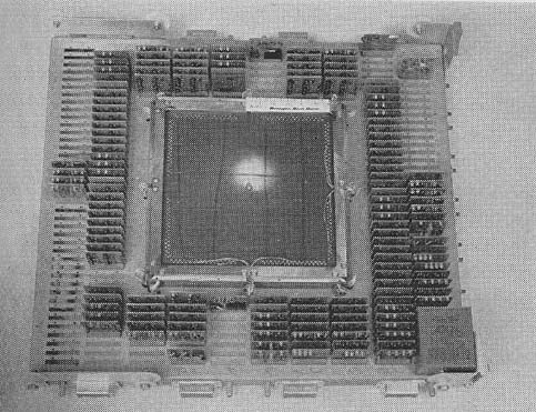
Fig. 8. One of the five separate memory chassis
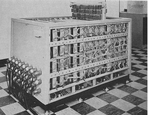
Fig. 9. The nine logic chassis and five memory chassis mounted in cabinet
The nine logic chassis and five memory chassis are mounted vertically in a "deep freeze" cabinet as shown in Fig. 9. The total volume of this cabinet is less than 2 cubic yards. The interconnections, between these chassis are made in the two side planes of the cabinet. The external equipment cables connect into the two end planes. Chassis are completely removable for test and repair. Standard auxiliary units shown with the computer in Fig. 10 are the maintenance console and the monitor typewriter. (The highspeed paper tape reader and punch are not shown). Other auxiliary units such as the magnetic tape and magnetic drum are presently being developed for use.
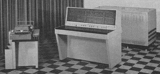
Fig. 10. Maintenance console and monitor typewriter
Many test programs have been operated, ranging from simple service and diagnostic tests to more complicated system operation with other equipments. Also, the M-460 has carried on a "conversation" with a magnetic- switch test computer, played musical tunes through its input-output section, and has performed a number of other unusual feats. The performance of the Univac M-460 leaves no doubt as to the excellent future of solid- state digital computers.
Reference
1. A PROGRESS REPORT ON COMPUTER DESIGN, S.
R. Cray, R. N. Kisch. "Proceedings of the Western Joint
Computer Conference," AIEE Special Publication T-85,
Feb. 1956, pp. 82-85.